Gate drive layout
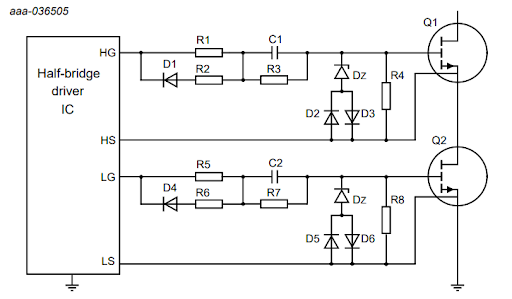
The actual gate drive is a litte more complicated than in my test layout. I’m using the circuit from AN90041, which looks like this:

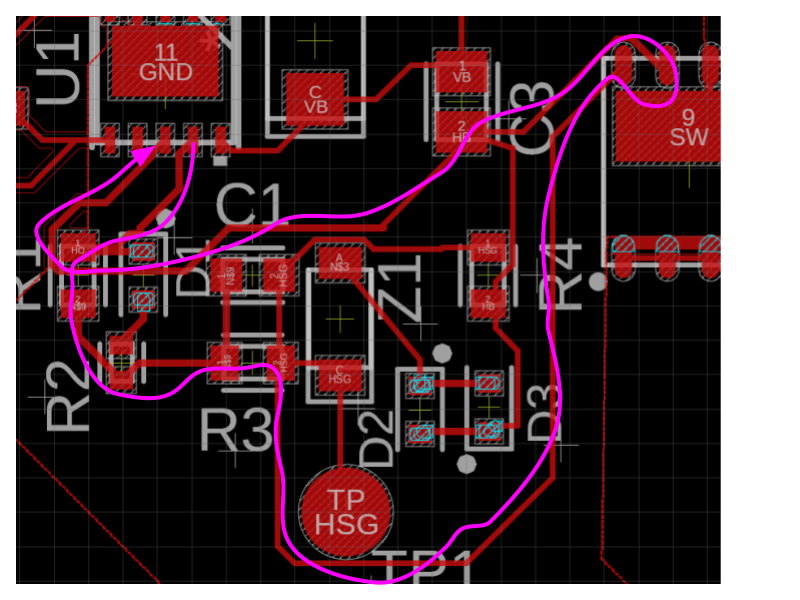
The crossing over of traces works about the same as in the test layout, though. Here’s one version of the high side drive, with a purple scribble showing the current path during the turn on transient:

So, that works. But how well? You know, there’s a lot of area enclosed in that loop. Enclosing area means making lines of magnetic flux, which means inductance. Inductance means oscillations, transients, spikes and losses.
How big a deal is this? Well, here’s what the NCP51820 data sheet has to say, as the Number 1 priority in routing a PCB for high frequency power switching:
Multi−layer PCB designs with proper use of ground/return planes as described in this document are a must. High frequency, high voltage, high dV/dt and high di/dt all warrant the need for a multi−layer, PCB design approach. Inexpensive, single−layer, PCB designs do not allow for proper routing or design of ground planes necessary to realize the full benefits of a GaN based power stage.
Uhh, that’s pretty rough. Sounds like the concept won’t work at all, at least not as single layer. Or maybe it just means it won’t realize the “full benefit”, and have to run at lower frequency or something.
How big is the inductance in this layout? We can estimate it. The squares are 1.0 mm, so the loop is somewhere around 14 x 14 mm. We also need the trace diameter for the calculator. The trace width here is 0.2 mm (8 mil), the thickness might be 0.1 mm (3 oz), so an equivalent diameter for a circular cross section of wire is 0.16 mm. The result is 4e-8 H = 40 nH.
Is that a lot? I’m not sure, but EPC WP009 has plots with power loop inductances in the single digit nH. This is a gate drive loop though. Nexperia AN90006 is also full of advice, but not much numbers, just says to minimize area to keep gate loop inductance small.
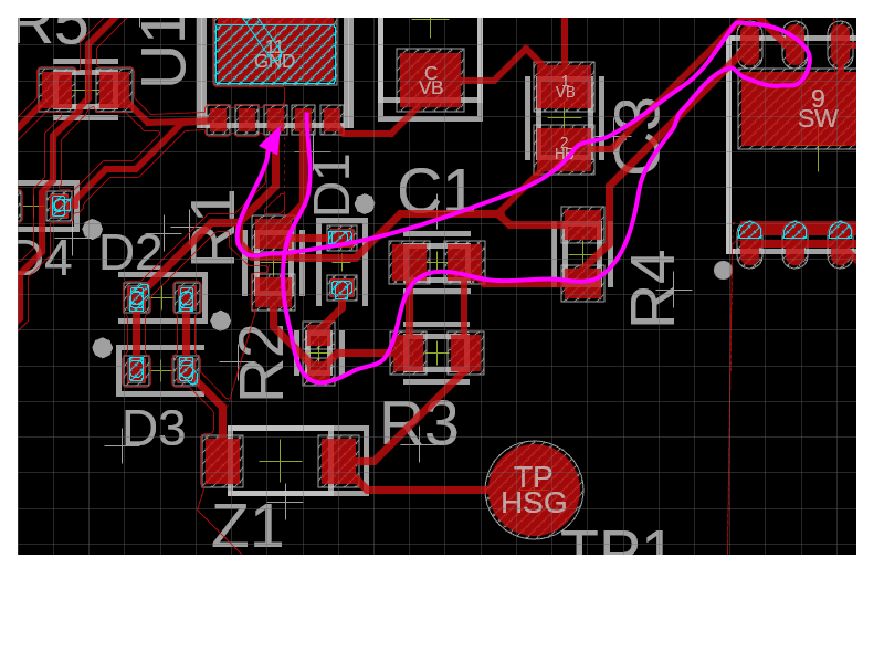
Would it be better as a trace over a ground plane? Another calculator for similar inputs (14 mm long 0.2 mm trace 0.2mm above plane) gives 4 nH, 10x lower. That’s significant. Other changes, like widening wires don’t do too much. One thing we can do without going to multilayer (which has thermal impacts) is moving components outside the loop, so the loop encloses less area:

Skinnier, should be better, even if not as good as a multilayer PCB.