Single layer test layout
A reasonable question after picking a whole bunch of appealing design rules is whether you’ve argued yourself into an unfeasible position. Single layer is a strong constraint. I note that the Nexperia sample PCB is certainly not single layer, nor is the sample layout in the NCP51530 data sheet. Single layer layouts can be a little complex, global geometry optimization problems. However, you have lots of components which can kind of act like jumpers to put a trace under, and flexibility as to where you put connectors, etc. You can add more zero resistance resistors if you need more jumpers, too. We also need to meet voltage clearance constraints, plus all the other requirements and recommendations for the circuit. I figured it’d be a good idea to try a test layout of a simplified version just to see if the rules were already too restrictive.

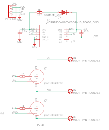
For a circuit, I simplified the gate drive to a single 0805 gate resistor, so I’d have one jumper to work with. The bootstrap and decouplng are I think reasonable. For power input and output, I just have 3 separated mounting holes. Low voltage inputs are collected together.

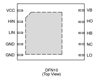
The gate driver has inputs on the left, outputs on the right, with a bit of gap between the high voltage pins and the thermal pad.

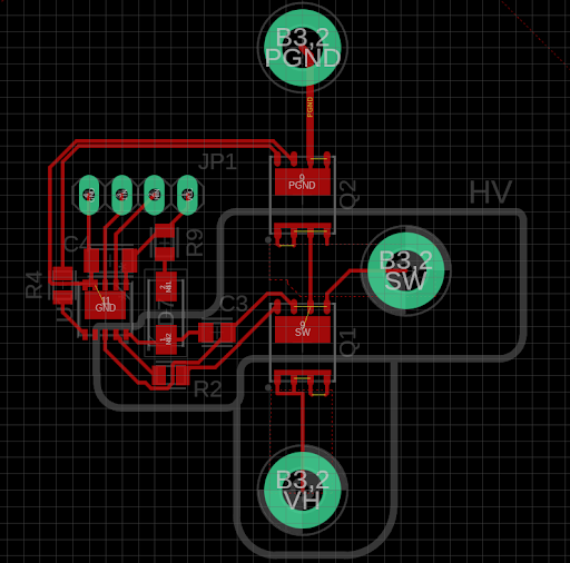
Here’s one way to lay this out. I put the gate driver on the left so the signals could go left to right, but because of where the gate and Kelvin source pins are on the FETs the high side ends up on the bottom and the low side on the top. Seems a little awkward, but that’s how Nexperia’s example did it. The high side gate and return have to switch positions, using the gate resistor. Seems straightforward. The low side gate trace, on the other hand, has to wind around the whole circuit, distance of ~30mm. Not ideal, but not clear there’s a better option. You can’t go under the gate driver, because of the voltage clearance required. And I think you want low voltage traces to entirely avoid high voltage areas, because otherwise meeting clearance and creepage is annoying. Two separate high voltage areas are marked. The barriers are only crossed by devices intended to withstand voltage. The overall result isn’t beautiful or final, but I think it does show that single layer isn’t too strong a constraint. At least, not yet.