It looks stupid and I feel stupid


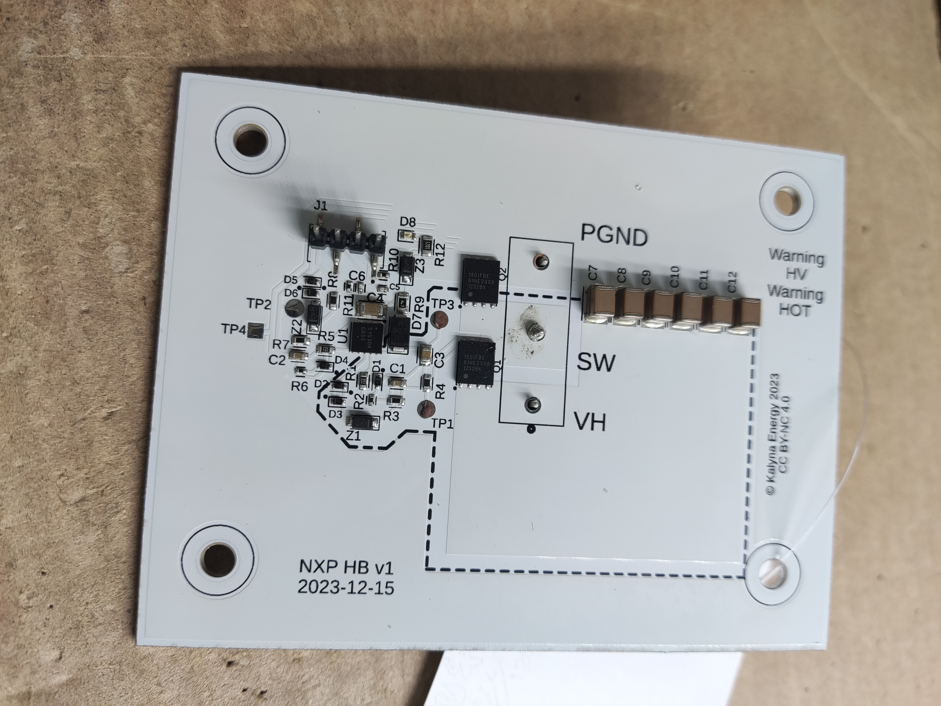
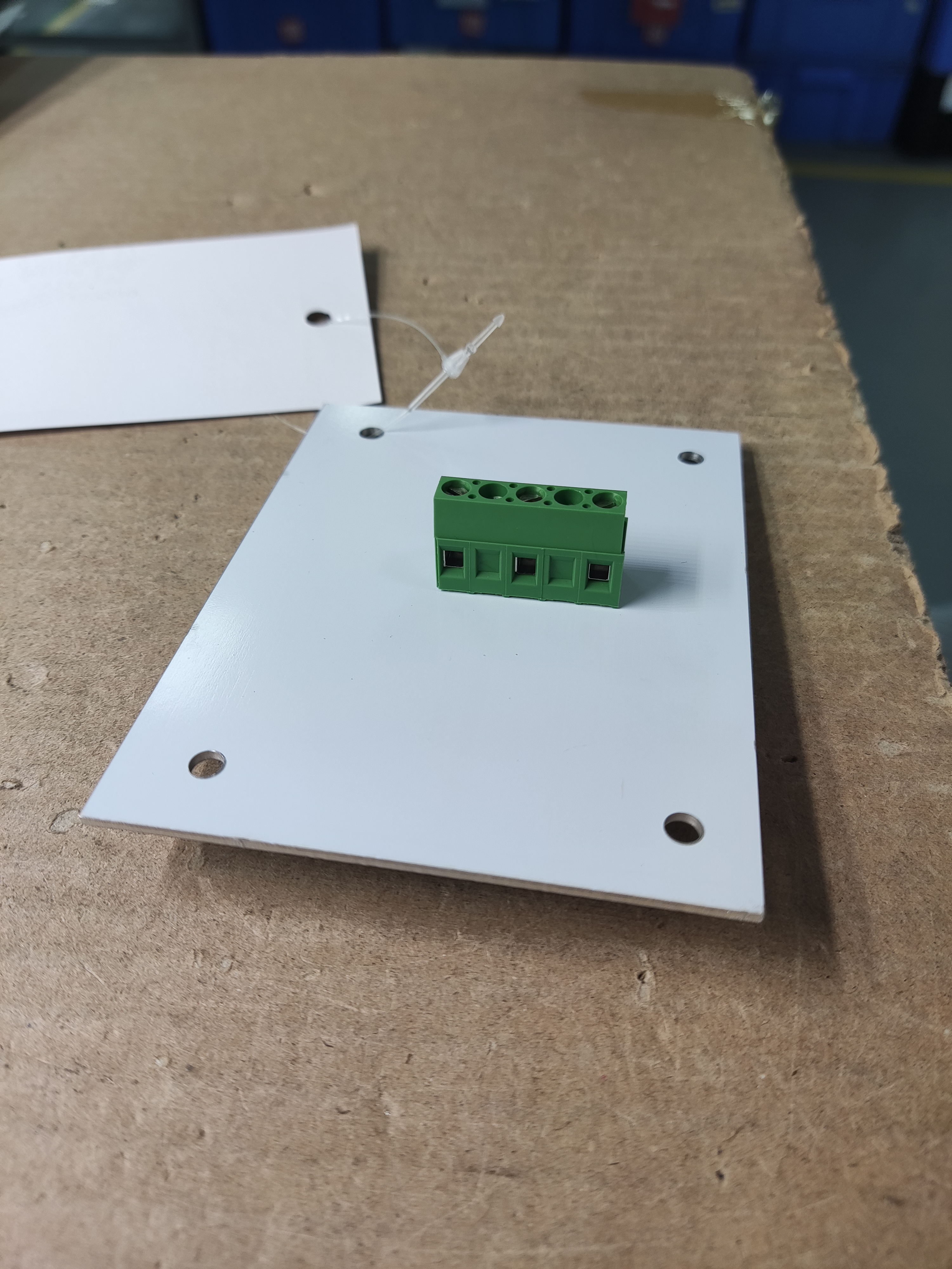
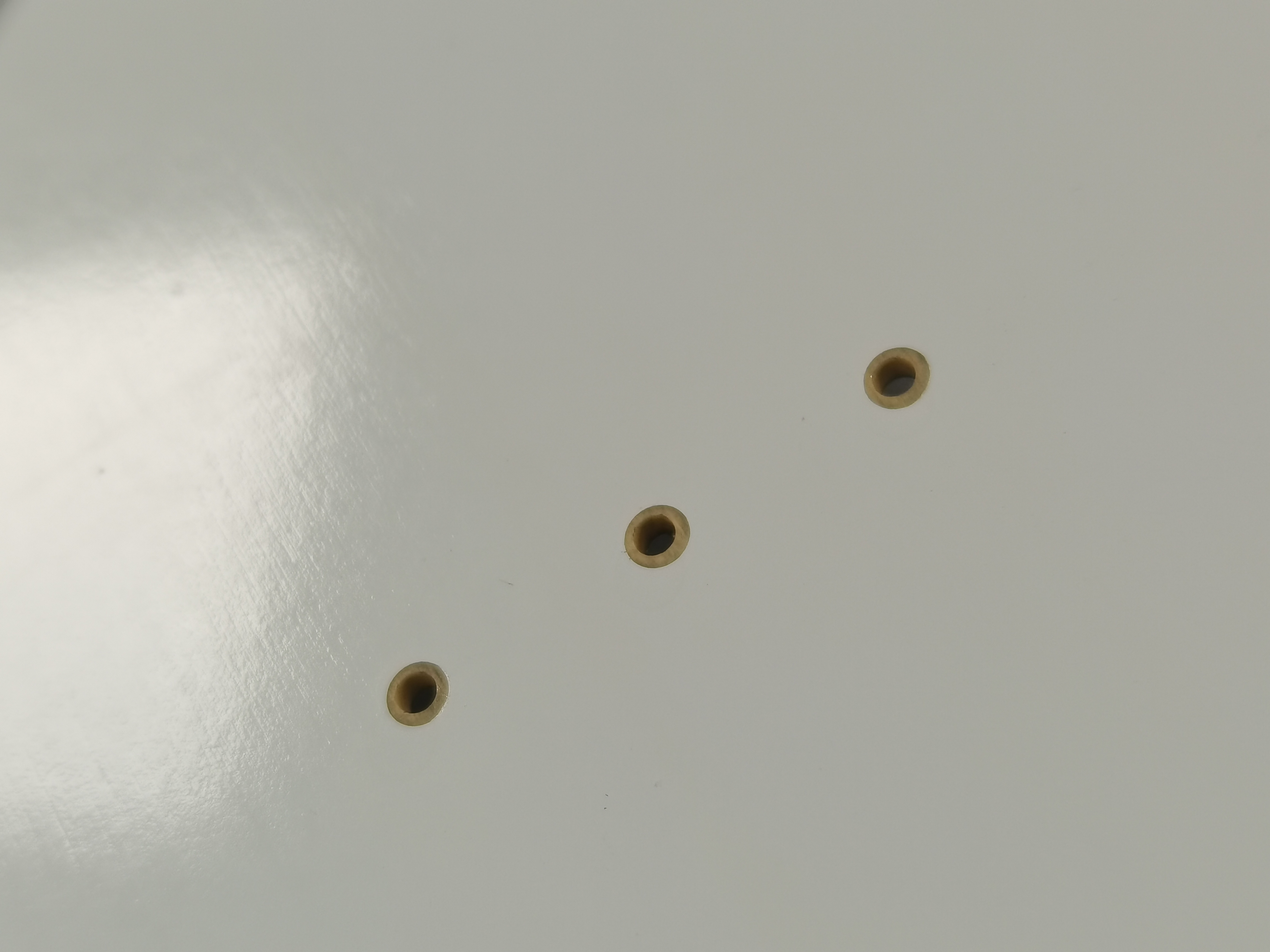
Here is a test assembly. As you can see, the power connector terminal block has been placed on the bottom. That’s not what I intended. However, it can’t be soldered onto the top side. Here is a detail of the bottom side:

There are no pads for the leads to be soldered to. They were present in the footprint for the component, but were the only features on the bottom copper. I thought they weren’t needed, and was trying to design a single-sided board. So I deleted the bottom copper gerber, and ordered a single sided board. Now, I guess I’m going to get a board with a terminal block on the bottom. I guess that can work too, but I feel stupid. Screwing up is how we learn things, though.