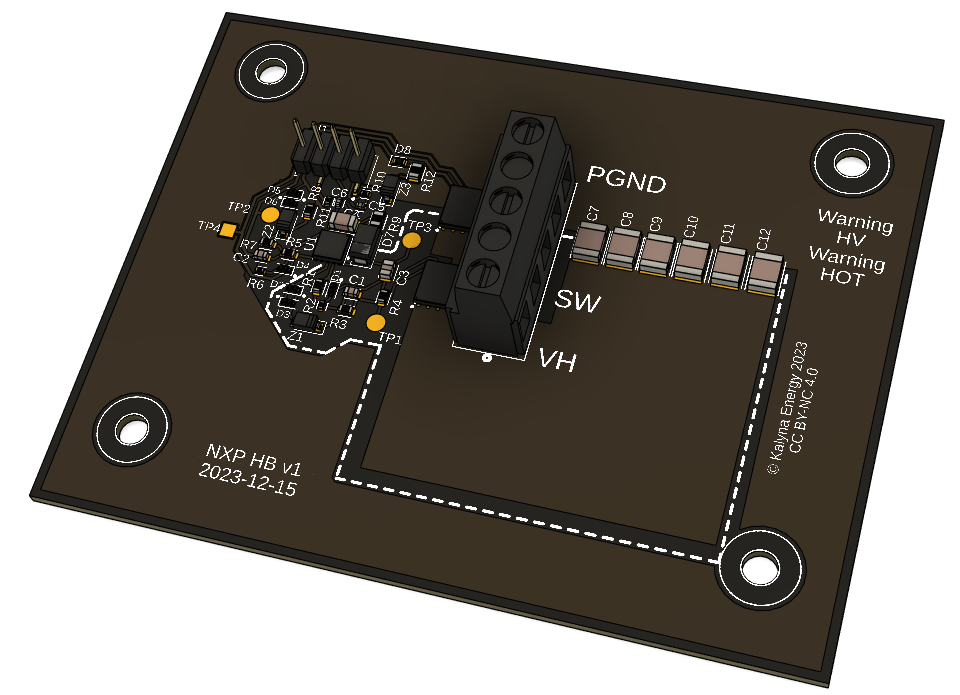
Half bridge prototype ordered
So I successfully finalized the layout and placed an order. It’ll look something like this:

The goals for this board were as follows:
- Review how to do layout and use the software
- Have a board to physically evaluate some interesting new parts (Nexperia’s 650V e-mode GaN FETs)
- Understand better the advantages and limitations of metal substrate boards, and get experience having them built
- See if a single layer layout is possible
- Start making the mistakes that will help move the project forward
- If everything works well, use it to build some bench circuits for different topologies
- By creating a physical artifact, help the project feel more real both to myself and others
It was never supposed to be a final board that could be used in applications, but I did try to avoid things that would make this impossible.
I’m expecting at least coin flipping odds it won’t work at all, due to making some error somewhere. I’m hoping it’ll be possible to at least figure out where the issue is, so that I can iterate. But there’s an even higher probability, say 90%, that it won’t satisfy all of the goals above. In particular, compromises made to satify one objective (try manufacturing a metal board) may be incompatible with others (have an ideal platform to evaluate a particular device). It may turn out to be well and thoroughly optimized, but to the wrong metric. Still, some of the goals have been achieved already: I’m now current on the PCB layout tool, single layer IMS is possible, putting through hole components on IMS is possible (but adds cost). And, while I’m waiting for the boards, I can work on what tests I will do when they arrive.