Bypass capacitors

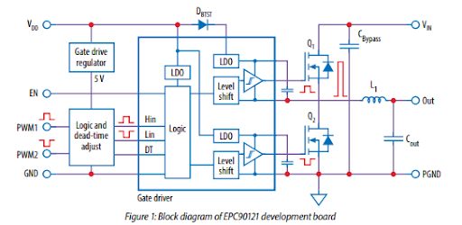
Here’s the EPC90121 block diagram, showing onboard power bypass capacitors. These are important, because you don’t want inductance in the power loop. It can lead to ringing, increasing switching losses, give spikes that damage components, etc. Some is unavoidable, but you’d like to reduce it as low as possible.

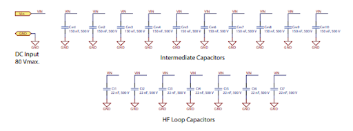
Here’s the schematic of how they implement that. They have two sets of capacitors, both X7R from the same series. One is a set of 0805 caps at a lower value, the other is a larger set of 1210. Total capacitance is about 1600 nF, 500V cap ratings, for a board rated to 280V 4A continuous at high switching frequency. Presumably the smaller caps have lower inductance, in their packaging or placement, enough so that the designers included them. I don’t know by how much though.
I figure it’d be a good idea to have some onboard power loop capacitance as well. It doesn’t stop the user from putting a significant energy storage capacitor off the board, but they can’t add low inductance capacitance. Better to give them some.
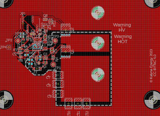
Our board specs are different from the 90121. The purpose of the board is to test the gate driver and fets, which are 650 V 11 A high frequency parts. Supporting the exploration of these capabilities, as much as reasonably possible, is the goal. So the caps should be rated for a higher voltage than the 90121 caps, probably 1000 or 1500 V. 1000 V is a reasonable number, more than 2x a bus link voltage of 400 or 500V, and still provides some factor above 650 V. In the same series, this needs an 1812 package size. Kemet has a series called Konnect which offers stacked caps, up to 200 nF at 1000 V in 1812. I’m not sure how much capacitance is required, it probably depends on lots of things which I don’t know. But more is better, and there’s room to stick a few in. Here’s one possible layout, with 6 200 nF caps for a total of 1200 nF onboard bus capacitance:

I put the caps away from the VH power connector pad, thinking that we need clearance for high voltage between bare conductor at the connector and bare conductor on the cap terminals.
Now let’s think about power loop inductance.

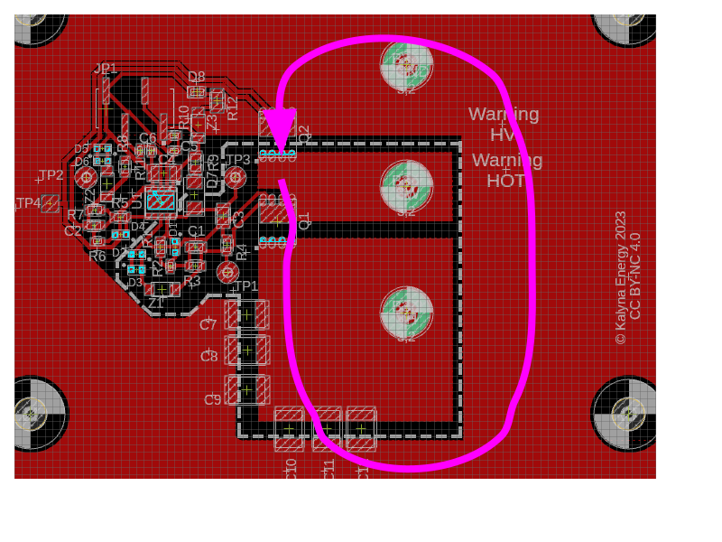
Here’s where the high frequency transients through the circuit have to flow. Power comes out of the caps, goes around the power connectors, and flows through the fets to whatever the circuit is doing. There’s a fair bit of area enclosed by this loop, creating parasitic inductance. Some of the power will flow the other way, but the area is about the same. It does help, because that inductance is in parallel. Still, it looks suboptimal. It might be possible to move the SW node connector and limit the loop size, but some clarification about what the clearance requirements are would be necessary. I’ll leave this for a separate post.