PCB layout rules
While doing the layout, one must determine what manufacturing constraints are present. These will be some combination of technically feasible, economically feasible, and technically required.
For this project, I’m hoping to use an aluminum core PCB. Reasoning: mechanically strong and stiff, so it might form part of (or all!) of the product housing. Conductive, so can form part of (or all!) EMC shielding. Highly thermally conductive, so can help reduce (or eliminate!) the need for other heat sinks. Lots of expectations here.

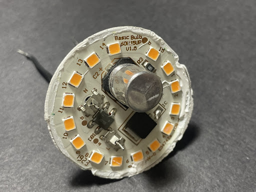
Here’s the PCB from a low cost LED bulb. This device is part of the inspiration for the whole project. It’s clearly extensively optimized for cost (just a few parts) but can interact safely and efficiently with line power. The entire bulb retails for a couple of bucks. This is a load, not a source, and lower current/power than we’ll be aiming for, but still, philosophically, perhaps a useful model design. This is a single sided aluminum PCB, 1.0 mm thick, with a single ~1 oz copper layer. It dissipates perhaps 10W total.

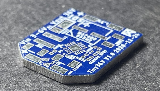
This is a small DC-DC converter we built for a client, also done as a single layer aluminum PCB.
One approach is to look at what vendors quote as easy and cheap, vs expensive. The idea is that whatever is cheap and fast is likely to be technically and economincally feasible, reasonable compromise, and popular among people doing similar things. I went onto PCBWay’s pricing calculator, and found the following set of parameters are cheap and fast:
- 1.6 mm, 1.5 W/(m K) aluminum core
- single layer
- black on white or white on black silkscreen and solder mask color, just top or both sides
- 8/8 mil (0.203mm) min track width and track spacing
- 2-4 oz copper
- HASL w lead surface finish
- 0.8mm min dia holes
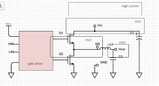
To this we should add separation between nodes with high relative voltages. We have a few of these:

The whole domain of adequate creepage and clearance is complex, but from IPC calculators like this and looking at boards, I think 2.0 mm separation will be pretty good: 375 V for bare conductor, 850+ V for internal or coated leads or conductors.
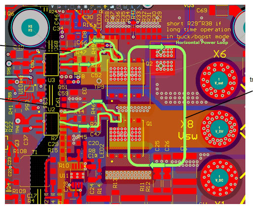
We also need to worry about inductance and resistance of traces. Basically, shorter, wider, and thicker is better. Details matter, but depend on frequency.

Nexperia’s example from AN90041 uses polygonal pours 8mm+ in width. HV feature separation appears to be about 1.0mm but it’s not clear what layers they are on, nor what voltage limit this board was laid out for.