A four switch boost inverter?
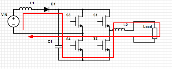
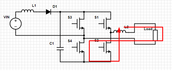
Awhile back I came across the following inverter topology:

The authors claim that it supports voltage boost, bidirectional output, common ground (avoiding leakage current) using only four switches. Given the purpose and philosophy of this project, you can see why this would be interesting to me. I have some familiarity with the literature (Khan 2020 is a decent review), but this topology looks new to me. It’s a little surprising to see new topologies, especially simple ones, appearing now. Also, parts of the circuit make no sense to me, I couldn’t make much sense of the text, details of the simulations and experiments seem thin, and (although I shouldn’t really look at this) the authors’ institution and the journal ranking are modest at best. So, I’m skeptical. Still, as an exercise in circuit analysis, I can try to prove that this circuit couldn’t do what it claims to.
(As a side note, even if it can work, that doesn’t mean it’s optimal for our purposes. There are metrics more important than switch count.)
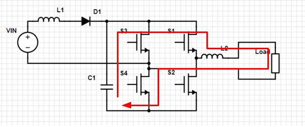
The first thing I noticed is the cap and diode in series in the center, labelled C1 and D2. This has to be an error, right? The cap will charge, when power is connected, but can never discharge due to the diode. It’s hard to see how current flowing here can aid the circuit. Even if there was some role for that current path, it’s equivalent to the path of C2 followed by the body diode of S4. So it seems redundant or pointless, and I don’t understand why it’s there. Accordingly, I left this out and redrew the circuit:
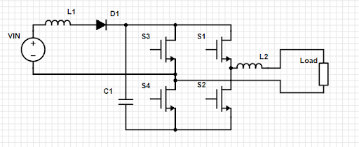
The section to the right of D1 looks like a full bridge inverter, supplied by a DC link energy storage cap C1, with an inductor L2 to filter the output. Normal enough. On the left we have our voltage source, hooked to the top of our bridge through an inductor L1 and diode, but with the bottom connected not to the bridge bottom but instead to the switch node of the left half bridge. This kinda looks like a wiring error, but it can’t be an error, because we need input ground directly connected to output ground in order to be a common ground inverter. (See Khan for why common ground is desireable for PV inverters, it has to do with parasitic capacitance of the panels and leakage oscillations with the output filter inductor.) So the question is whether we can charge and maintain C1 at the desired level during all phases.
We can explore the topology by tracing current paths. By counting connections and using Kirchoff’s current law, we can see there are four independent current loops in the circuit. We don’t need to talk about switch modulation strategies or component values just yet, let’s just see where currents could go, and try to tell a story about each current loop. First, let’s look at four current loops including VIN. Note some of these loops may end up redundant with combinations of other loops we’ll look at later.
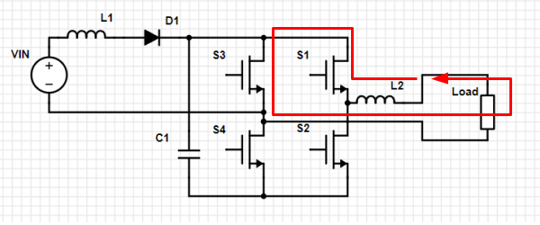
Loop 1. Switch S1 is closed, other switches are open. Current builds in L1 and L2, if we start from zero. Current flows through the load in the positive direction. This current path does not affect charge on C1. Because of D1 this current must be positive (looking at this loop in isolation).
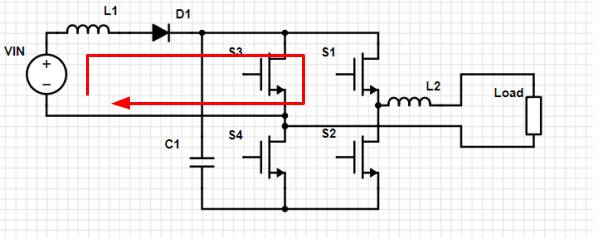
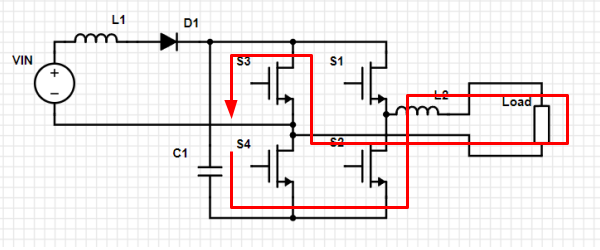
Loop 2. S3 closed, other switches open. Current builds in L1. Whenever S3 is closed, this loop will be active, building energy in L1 which can be used for the voltage boost.
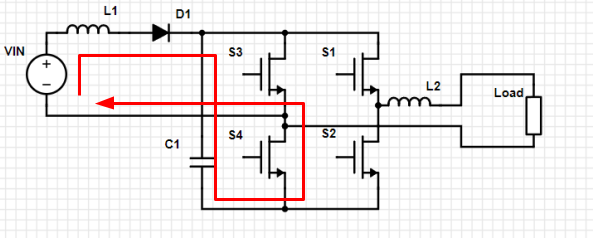
Loop 3. All switches open, but reverse current flows through S4. (I’m assuming all switches do not block reverse current, like a FET with a body diode.) Charge builds on C1, current through L1 may be increasing or decreasing as the voltage across C1 increases. D1 allows the voltage on C1 to be higher than VIN at zero current, so this current can’t go negative (in isolation).
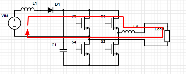
Loop 4. All switches open, but reverse current flows through S2. Positive current through L2 and load. Charge builds on C1. As for why the current would do this, rather than Loop 3, consider if we’re running current through L2 in Loop 1, then open S1. To keep the current through L2 flowing, it’ll suck charge through S2, even if it has to charge C1 in the process.
A couple of those processes charge the cap C1, which can now end up delivering current. We now look at four current loops driven by C1.
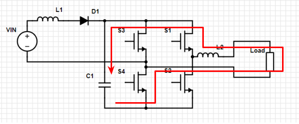
Loop 5. S1 and S4 closed, others open. Current can flow from C1 through load in positive direction, building current in L2, depleting charge on C1. This is a normal positive cycle for a full bridge.
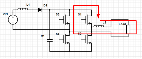
Loop 6. Charging positive. All switches open. S2 and S3 conduct in reverse direction. Positive but declining current in L2 turns into increasing charge on C1, transferring energy between L2 and C1 during a positive current cycle.
Loop 7. S3 and S2 closed, S1 and S4 open. Current flows through L2 and load in negative direction. This is normal looking reverse current direction from a full bridge, supplied by the C1 cap.
Loop 8. Charging during negative phase. All switches open. S1 and S4 conduct in reverse direction. Negative and declining current in L2 feeds increase of charge on C1.
It’s clear these loops are redundant, Loop 1 minus Loop 3 equals Loop 5, for instance, but the point is to be able to tell a story about what’s happening.
Is this all possible loops? Not quite. We also have loops of just the load inductor discharging, which are possible when any individual switch is on. There are four of these.
Loop 9. S1 is on. Forward current discharges through load, S3 (reverse) and S1.
Loop 10. S3 is on. Reverse current discharges through S1 (reverse), S3, and load.
Loop 11. Negative current through L2 discharging through load.
Loop 12. Positive current through L2 discharging through load. Will be present whenever S4 is on and L2 current is positive.
A table may be useful:
| S1 | S2 | S3 | S4 | Load current | Cap current | Active paths |
|---|---|---|---|---|---|---|
| 0 | 0 | 0 | 0 | pos | charge | Loop 6, Loop 4 |
| 0 | 0 | 0 | 0 | neg | charge | Loop 8 |
| 0 | 0 | 0 | 0 | 0 | charge | Loop 3 |
| 1 | 0 | 0 | 0 | pos | 0 | Loop 1 |
| 0 | 0 | 1 | 0 | 0 | 0 | Loop 2 |
| 1 | 0 | 0 | 1 | pos | discharge | Loop 5, Loop 1 |
| 0 | 1 | 1 | 0 | neg | discharge | Loop 7, Loop 2 |
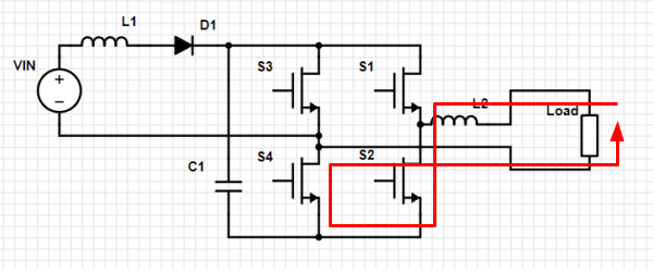
| 0 | 1 | 0 | 0 | neg | 0 | Loop 11 |
| 0 | 0 | 0 | 1 | pos | 0 | Loop 12 |
| 0 | 1 | 0 | 1 | either | 0 | Loop 11 or 12 |
This doesn’t quite cover all possibilities, nor is it entirely consistent, but it’s a start.
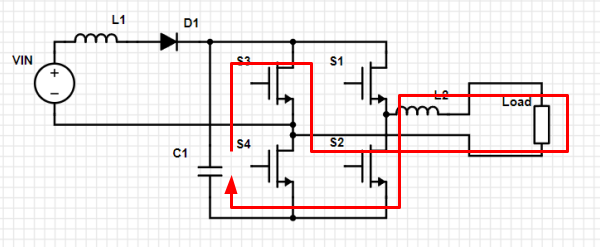
All right, so how could this work? Well, consider toggling S3 on and off. From the point of view of L1, this switches back and forth between Loop 2 and Loop 3, building charge onto the cap. There’s no limit on how much charge can be built up, so the cap can have whatever voltage you want, until you stop toggling. Here’s the cycle:
This is a little funny compared to a more usual boost:
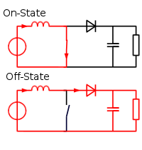
The standard circuit switches the inductor to ground to build current, then opens to force the current up through the diode and load. In our circuit, we have not two but three switches in series (counting the diode as a switch), with two intermediate nodes. The power is connected across the top and the lower intermediate node, and when the switch S3 opens current is forced onto the capacitor bringing the lower rail below the power ground. We need a negative rail, and this is how it’s generated for this circuit. If the voltage across the rails is a lot higher than VIN, VIN and L1 won’t be able to supply current for very long before the diode D1 cuts the current off.
Let’s talk about the full bridge inverter side again. One way to think about a full bridge inverter, with a given fixed voltage supply across the top and bottom rails, is that the bottom rail is the ground reference and both output terminals float relative to ground. On the positive cycle, S1 closes, connecting the positive load terminal to the positive rail; S4 closes, connecting the negative load terminal to the negative rail; and positive current flows through the load. Current can be controlled by opening the switches. In the negative cycle, S2 and S3 close, so the positive and negative load terminals are now connected to the negative and positive rails respectively, and current flows in the reverse direction through the load. This framework is useful when thinking about loads of motor windings, for instance. Closing S1 or S3 lift the positive or negative load terminal to the positive rail. The rails are not moving, only the floating load terminals.
Here, however, we’re in a framework where we’d like to use the negative output terminal as the voltage reference, and it’s probably physically connected with actual earth ground. Now, it’s the rails that are moving. In the positive cycle, S4 is closed, pulling the negative rail to earth ground, which shifts the positive rail to VDC above ground. S1 closes, connecting +VDC to the positive load terminal and positive current flows. In the negative phase, S3 closes, connecting the positive rail to ground, shifting the negative rail to -VDC below ground. S2 closes, attaching the positive load terminal to the negative rail at -VDC, so negative current flows through the load. Nothing physically is different if the system is isolated, just the language we use to describe the scenario. We do have to be a bit careful, because if our controller circuitry is referenced to the negative rail, its reference will be shifting relative to earth ground at high frequency.
I think that’s it for the moment. So far, I’m not completely convinced this circuit works, but I’m not convinced it can’t either.